INDUSTRY INSIGHTS
What File Type is Used for PCB Schematic Drawings?
Engineers usually start a circuit design with a schematic. Symbols represent components, and lines show how currents and signals move through the system. The drawing may look simple, but the file behind it carries the structure that design tools rely on every day. When a project moves from concept to prototype, teams often pause and ask a practical question: What file type is used for PCB schematic drawings, and how do those files move into manufacturing workflows?

Why PCB Schematic File Types Matter in Manufacturing
A schematic drawing describes the electrical logic of a circuit, while manufacturing teams build from production files generated later in the design process. The schematic file still plays a central role because it defines how components connect and how signals move across the design.
Inside that file is the connectivity data that drives the workflow from design to fabrication. When engineers transition into PCB layout, the design software converts schematic nets into physical traces and component placements. If file structures break or translation errors occur, the layout stage can inherit incorrect connections or missing references.
That situation slows prototype builds and leads to time-consuming troubleshooting.
Well-structured schematic files help engineering teams maintain consistency as designs move between CAD tools, layout environments, and manufacturing partners. Clear file organization also makes documentation easier to interpret when prototypes reach
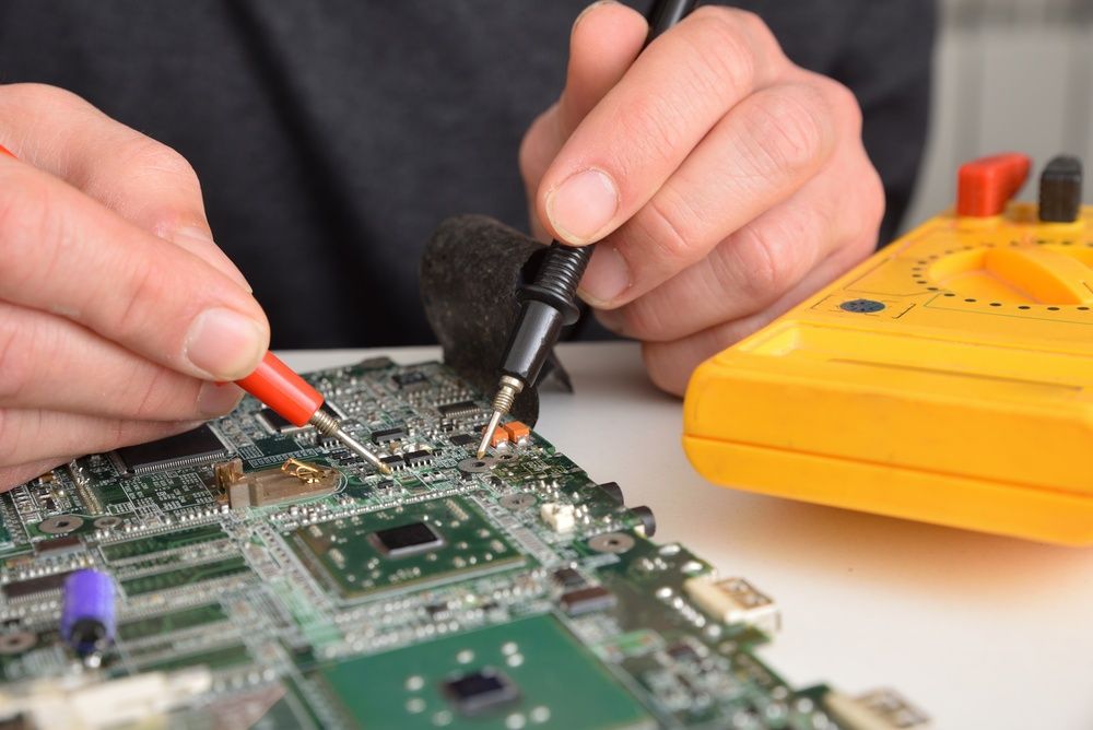
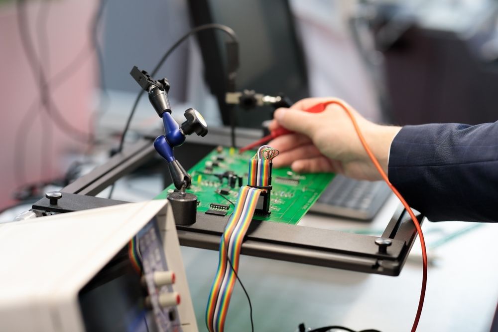
printed circuit board (PCB) assembly and testing.
Common File Types Used for PCB Schematic Drawings
There is no single universal format used across all schematic capture tools. Most engineers create schematics inside specific PCB design platforms, and each platform stores drawings using its own native file structure. These files contain more than symbols and wires. They hold connectivity data, component references, and links to part libraries used later in the layout stage.
Several file types appear frequently across the industry:
.DSN
Used by OrCAD Capture for schematic designs
.SCH
The standard schematic format used in KiCad projects
.CIR
Sometimes used in circuit simulation environments
.SCH/.SCHDOC
Common in Altium Designer projects for schematic sheets
.PRJPCB
Altium project file that organizes schematic documents within a design
ASC
Used by LTspice for schematic capture and circuit simulation
Each format preserves the circuit’s electrical relationships so design tools can translate the schematic into a physical PCB layout.
Native Schematic Files from PCB Design Software
Most schematic drawings start inside dedicated PCB design platforms. These tools combine schematic capture, simulation, component libraries, and layout features in a single environment. The schematic files created there store the electrical relationships that define the circuit.
Each platform uses its own native file structure to hold schematic sheets and project data. Common examples include .SCHDOC files in Altium Designer, .DSN files in OrCAD Capture, and .SCH files in KiCad projects. These files store symbol data, net connectivity, reference designators, and links to component libraries used later in the layout stage.
Because these formats belong to specific software platforms, engineers typically share them within teams using the same design tools. When collaboration expands to manufacturing partners or external groups, engineers often export additional documentation formats so the circuit structure stays clear throughout the prototype workflow.
Neutral File Formats Used for Sharing Schematics
Engineering teams often collaborate across different design environments. In those situations, native schematic files may not open correctly on another platform. Neutral file formats help teams share circuit information without depending on the same PCB design software.
One common option is a PDF export of the schematic. This format captures the visual diagram so engineers, technicians, and manufacturing partners can review component relationships and signal paths during design reviews or assembly troubleshooting.
Another widely used format is the netlist file, which describes how components connect electrically within the circuit. Many CAD tools export netlists that other layout systems can import when transferring a design.
Some environments also support EDIF (Electronic Design Interchange Format), a long-standing standard for exchanging schematic data between electronic design tools.
How Schematic Files Connect to PCB Layout Files
A schematic drawing captures the electrical logic of a circuit, while the PCB layout defines its physical structure. The link between the two runs through the design software used during development.
Once a schematic is complete, the CAD system generates connectivity data, often called a netlist. This information maps each component and its electrical connections. The layout environment then uses that data to place components on the board and route copper traces that match the schematic relationships.
Component footprints from part libraries connect schematic symbols to their physical packages. As placement and routing progress, the design gradually resembles the finished board.
When layout files are finalized, the system generates manufacturing outputs such as Gerber layers, drill files, and placement data used during
PCB assembly and fabrication.
How to Prepare Schematic Files for PCB Prototyping
As a design approaches PCB prototyping, schematic files should be reviewed and organized before fabrication and assembly begin. A structured preparation process helps engineering teams move from design to hardware with fewer issues.
Common preparation steps include:
1. Verify reference designators.
Each component should have a unique identifier that matches the Bill of Materials and layout files.
2. Confirm net connectivity.
Power rails, signal paths, and ground connections should reflect the intended circuit behavior.
3. Link symbols to the correct footprints.
schematic symbol should reference the physical package used in the PCB layout.
4. Export readable schematic documentation.
A clear PDF helps technicians interpret the circuit during fabrication and testing.
5. Validate component data for automated assembly.
Accurate part data supports equipment used in surface mount technology (SMT) in PCB assembly.
Need a PCB Prototype Fast? Call Ninja Circuits
At some point, every design leaves the screen and becomes hardware. Schematics turn into layout files, manufacturing data, and eventually prototype boards. That stage often reveals adjustments that refine the design before production.
Ninja Circuits works with engineering teams building early hardware versions of their boards. The company focuses on quick-turn builds and short-run production so developers can test ideas, troubleshoot circuits, and move projects forward without long delays. Their work centers on high-quality prototype assembly that supports real engineering iteration.
If a schematic has passed design review and layout files are ready, the next step is straightforward.
Contact Ninja Circuits to request a quote and start your PCB prototype.
INDUSTRY INSIGHTS