INDUSTRY INSIGHTS
A Comprehensive Guide to Printed Circuit Board Assembly
Printed circuit board assembly is where design becomes reality. It’s the stage where bare PCBs are populated with components and transformed into functioning electronics. These boards are the heartbeat of everything from wearables to aerospace systems. For engineers, this is where precision counts. A single misaligned part can derail an entire build, especially when working on tight deadlines or first-pass prototypes.
Successful PCB assembly hinges on clean data, proper material handling, and the right combination of surface mount and through-hole techniques. Add in quality control and final testing, and you’ve got a process that demands both speed and care.
At Ninja Circuits, we work with engineers every day to take clean files, fast-turn timelines, and demanding specs across the finish line. If your next project needs to go from concept to physical board with zero room for error, you’re in the right place.
What Is a
Printed Circuit Board (PCB)?
A printed circuit board (PCB) is the foundation of nearly every electronic device. It’s a flat, layered structure made of non-conductive material (usually fiberglass) with conductive pathways etched in copper. These pathways, also known as traces, connect components and allow electricity to flow through the circuit.
PCBs come in single-layer, double-layer, and multi-layer formats depending on the complexity of the design. At the core, their job is simple: organize and connect components in a way that makes the entire system work.
What makes a PCB “assembled” is the addition of electronic components, like resistors, capacitors, ICs, and connectors, that are mounted using automated machines or hand placement. Once populated, the PCB becomes the engine behind whatever the product is meant to do.
Key Components of a Printed Circuit Board
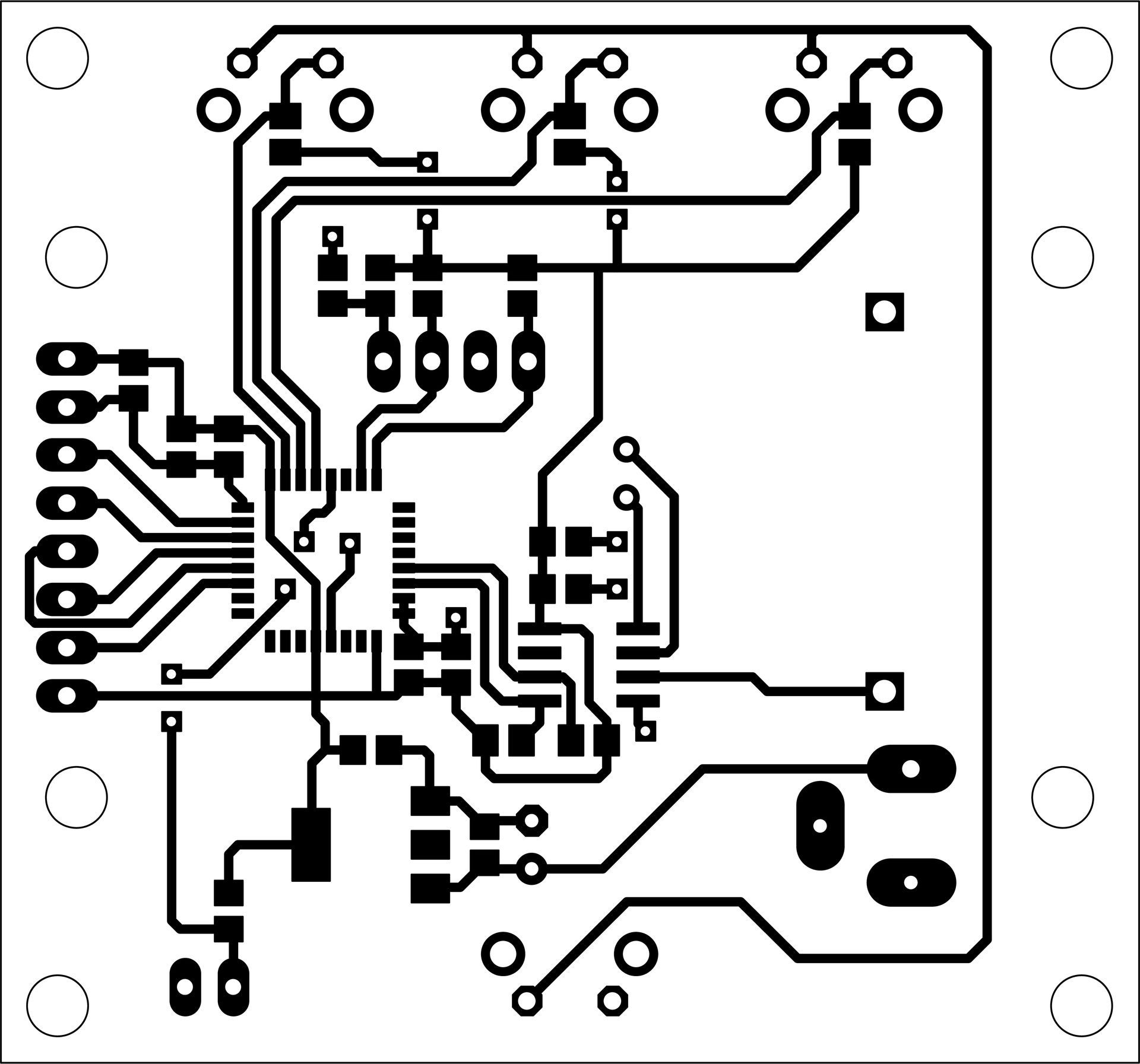
Every printed circuit board is built around a few essential elements that make the whole system tick. It starts with the substrate, usually FR-4, which gives the board its structure and strength. On top of that is the copper layer, where conductive traces are etched to route signals and power between components.
A solder mask is applied over the copper to prevent oxidation and bridge shorts, while the silkscreen layer provides printed labels to identify parts and reference points. These layers together form the bare board, but it’s the components that bring it to life.
Common components include resistors, capacitors, diodes, inductors, ICs, connectors, and transistors. Each plays a role in signal conditioning, power management, or logic processing. Placement, polarity, and spacing are critical, especially in high-speed or high-density designs.
Together, all of these elements come together to create a functioning circuit to power most modern electronics.
The PCB Assembly Process: Step by Step
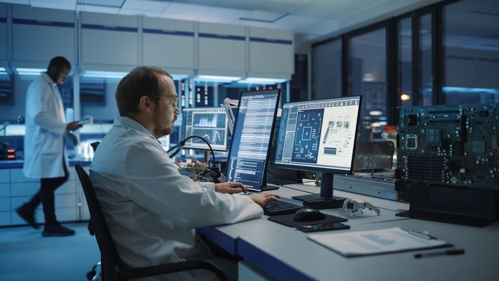
Printed circuit board assembly is a precise, multi-stage process that transforms a bare board into a functioning electronic system. It combines automation, engineering judgment, and strict process control.
Each step builds on the last, starting with clean, well-prepared files and ending in tested, production-ready boards. Whether you’re building surface mount, through-hole, or mixed-technology designs, the overall flow remains consistent: data in, components placed, solder joints formed, inspection completed.
At Ninja Circuits, we streamline this entire path with fast-turn capabilities and a deep focus on quality. Here's how it all comes together:
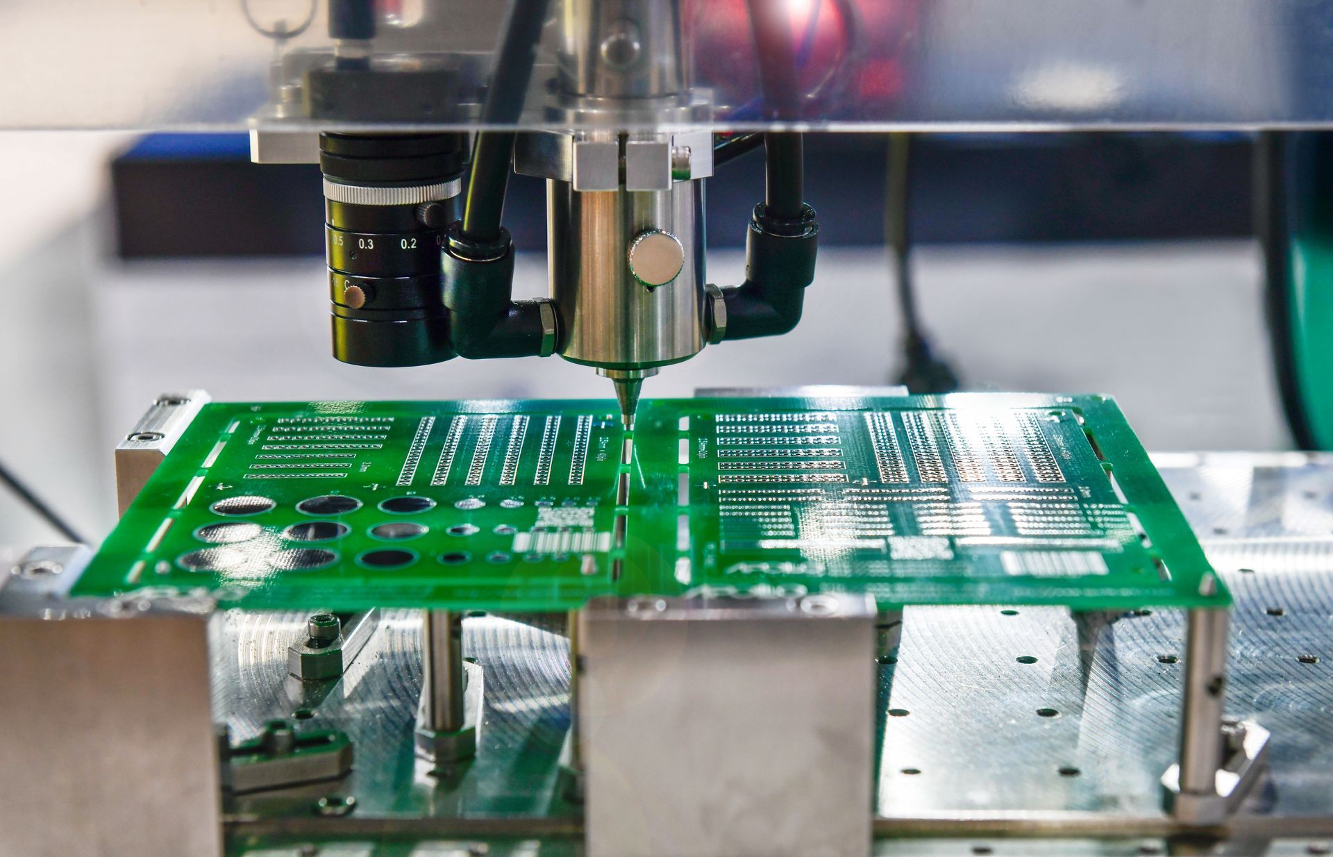
Design and File Preparation
Every successful PCB assembly starts with clean, production-ready files. This includes Gerber files, Bill of Materials (BOM) in Excel format, centroid data, and assembly drawings. Engineers also provide part placement preferences, special instructions, or callouts for critical components. At Ninja Circuits, we review files up front to catch red flags early and avoid mid-stream delays.
Solder Paste Application (Stenciling)
Solder paste, a mix of powdered solder and flux, is applied to the pads where surface-mount components will land. A stainless steel stencil is aligned over the board, and a squeegee pushes paste through the cutouts. This step determines the quality of every solder joint that follows, making precision and stencil cleanliness critical. Stenciling is the first part of the production process, and the most important.
Too much, or too little solder paste will affect the outcome of the entire build. Ninja Circuits designs each stencil specifically for every project, from a standard 3,4, or 5 mil stencil to the more complicated step stencils. All depending on what is needed for a successful build the first time.
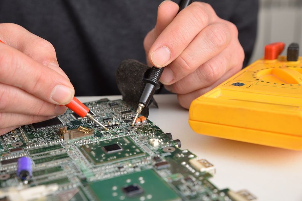
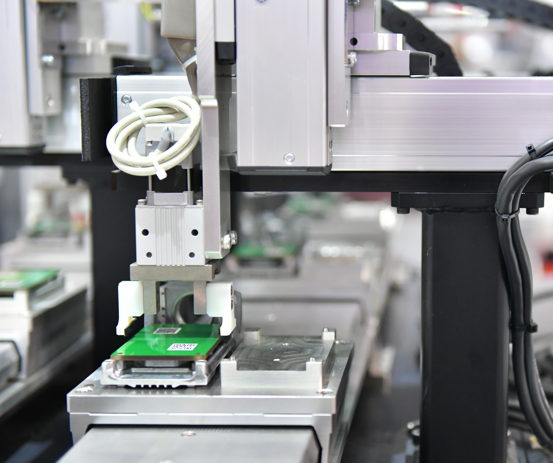
Pick and Place Machines
Once solder paste is applied, the board moves to high-speed pick and place machines. These systems use vision alignment and precision nozzles to accurately place surface-mount devices (SMDs) onto the board. Components are pulled from reels or trays, rotated as needed, and dropped into the paste with incredible accuracy, often within a tolerance of microns. This step defines placement integrity and directly impacts yield and rework rates. Ninja Circuits’ placement machines can place almost any SMT component available. This includes components as small as 01005 size to massive 3600 ball 4” square BGAs.
Reflow Soldering
After placement, the board enters a vapor-phase reflow system. Heat is carefully ramped up to melt the solder paste, creating strong electrical and mechanical connections between each component and its pad. Ninja Circuits uses vapor-phase reflow for precise thermal control on all our assemblies.
Inspection and Quality Control
Inspection catches what automation misses. Post-reflow, boards are scanned using 3D Automated Optical Inspection (AOI) systems to detect misplaced, misoriented, or missing components. For bottom terminated components, like a BGA, X-ray inspection will be used to inspect each joint.
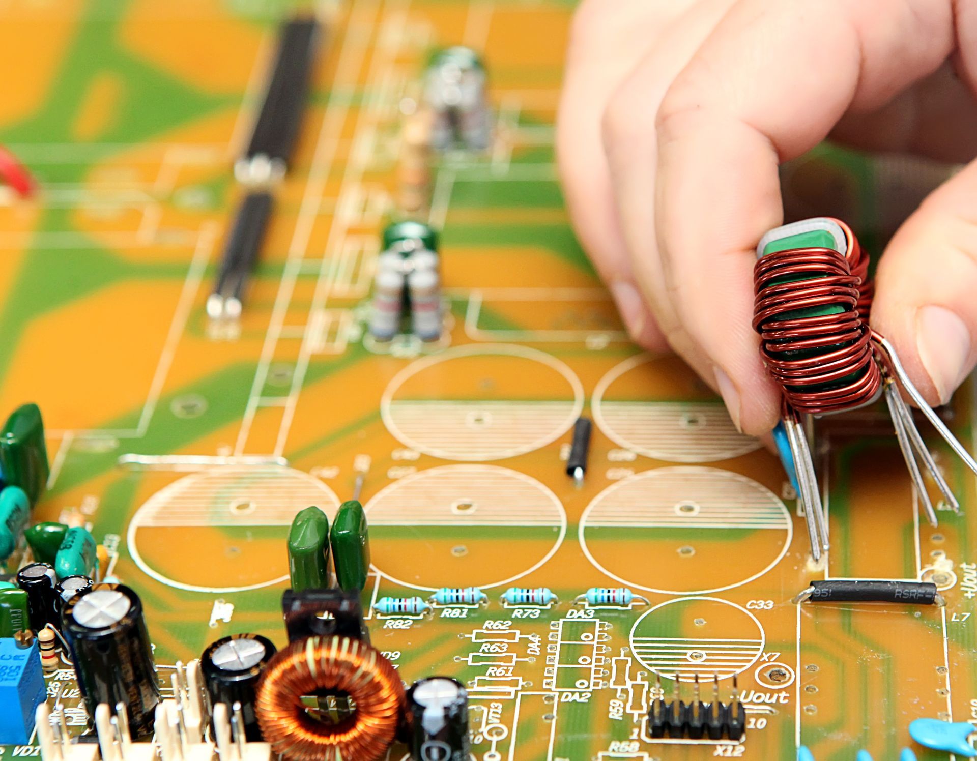
Through-Hole Component Insertion
For designs that still require through-hole parts, like connectors, transformers, or legacy components, these are inserted by hand or semi-automated equipment after surface-mount steps are complete. They’re soldered using wave soldering or hand soldering, depending on board complexity. Mixed-technology boards often require careful sequencing to avoid thermal or mechanical issues during final assembly.
Final Testing
Once all components are in place, Ninja offers the option of flying probe testing. The goal is to catch issues before the board hits a lab bench or field deployment.
What to Expect
Post-Assembly
At Ninja Circuits, boards ship clean, carefully packaged, and ready to use. If you’ve requested serial numbering, conformal coating, or special handling instructions, we can provide you with that. After shipment, we keep in communication with you after delivery. This is because feedback, design tweaks, or version changes are common, and we can help you there also!
INDUSTRY INSIGHTS