INDUSTRY INSIGHTS
The Significance of Thermal Management in PCB Design
Heat rarely appears on a schematic, but its impact shows up everywhere in real-world performance. It hides in current density calculations, compact layouts, and aggressive power targets. Early prototypes often power on and pass initial tests, which makes the temperature feel manageable at first.
Over time, though, longer run cycles, tighter enclosures, and limited airflow begin to compound. Components drift out of tolerance, signals lose margin, and reliability questions surface. That tension sits at the center of PCB thermal management, where early design decisions quietly shape long-term performance in the context of thermal management in PCB design.
Why Thermal Management Is a PCB Reliability Problem
Most reliability failures trace back to heat, even when temperature was not flagged as a primary concern during design. Elevated junction temperatures, uneven copper distribution, and concentrated hotspots quietly reduce operating margin long before a board stops functioning.
These patterns often become visible during
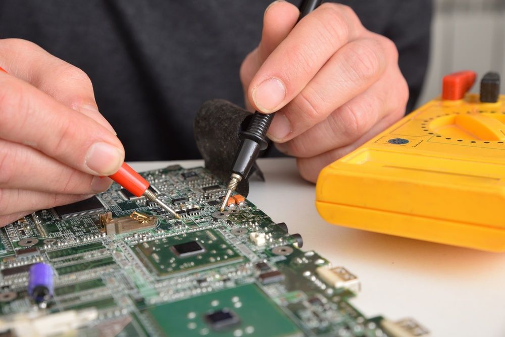
low-volume PCB assembly, once hardware runs under sustained load instead of short bench tests. Power devices settle into real thermal conditions inside enclosures. Dense component clusters begin interacting thermally. What seemed stable in early validation starts to drift, and in many cases, the root cause points back to thermal assumptions made early in the design process.
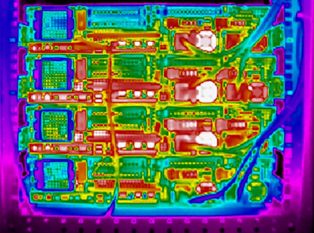
Primary Heat Sources in High-Density PCB Layouts
High-density layouts concentrate power in smaller footprints, which changes how heat moves through the board. Voltage regulators, FPGAs, high-speed processors, and power MOSFETs generate the most obvious thermal load, especially when current density climbs and switching frequencies increase.
Less visible contributors often matter just as much. Tightly spaced passives restrict airflow, and inner-layer copper planes can trap heat when they lack proper thermal paths to the surface. Even high-speed interfaces add incremental heating that compounds over time in ways that are easy to overlook during initial layout.
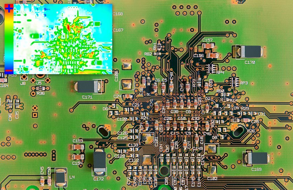
When these sources cluster in one region, temperature gradients form across the PCB. That imbalance influences component performance, solder joint stress, and long-term stability far more than many initial layouts account for.
How Excess Heat Affects Signal Integrity and Lifespan
Temperature influences electrical performance in subtle ways before failure becomes obvious. Rising heat increases conductor resistance, shifts impedance, and alters timing margins in high-speed designs. Oscillators start to drift, ADC accuracy moves outside expected ranges, and high-speed serial links lose eye height as noise margins shrink.
Over time, elevated temperatures accelerate material fatigue. Solder joints expand and contract through repeated thermal cycles, PCB substrates experience mechanical stress, and pads can lift. In extreme cases, vias may crack under sustained strain, leading to intermittent faults that are difficult to track down. When that happens in the field, you are often looking at
PCB repair instead of straightforward replacement.
What begins as a manageable hotspot can quietly shorten lifespan across the entire assembly.
Thermal Management in PCB Design Starts at Schematic
Thermal performance takes shape long before placement begins. Power budgets, component selection, and regulator topology all influence how much heat the board must dissipate. A linear regulator chosen for simplicity can introduce far more thermal load than a switching alternative. Current limits, duty cycles, and worst-case operating conditions belong in early calculations, not in a late-stage design review when options are limited.
Simulation helps, but assumptions need hardware validation. That is where
rapid PCB prototyping becomes part of the design process rather than a final checkpoint. Early revisions reveal how theoretical power dissipation translates into real surface temperatures, copper spreading behavior, and enclosure interaction. When thermal intent starts at the schematic, layout decisions become clearer, more deliberate, and less reactive.
Layout-Level PCB Thermal Management Techniques
Once placement begins, thermal intent turns into physical strategy. Component spacing, copper balance, and airflow paths start shaping how efficiently heat leaves the board. Small layout adjustments often create measurable differences in surface temperature, which designers quickly see in the lab.
Common layout techniques include:
Spreading high-power components apart to reduce localized hotspots
Avoiding isolated copper islands that trap heat instead of distributing it
Aligning heat-generating parts along natural airflow paths inside the enclosure
Connecting thermal pads to large copper pours to improve lateral heat spreading
Matching copper weight to the expected current density rather than the default stack settings
Placing temperature-sensitive components away from known high-dissipation regions
Thoughtful placement decisions at this stage reduce rework later and stabilize performance under sustained operating conditions.
Thermal Vias, Copper, and Stackup Considerations
Thermal control often comes down to how effectively heat moves through the board instead of across it. Copper weight, via density, and stack configuration influence vertical heat flow and overall temperature balance. A board that looks thermally stable on the surface can still trap heat internally if the stackup limits conduction paths.
Designers typically focus on:
- Adding arrays of thermal vias beneath power packages to transfer heat into internal planes
- Increasing copper weight on power layers to improve heat spreading capacity
- Connecting internal planes to surface pours to reduce temperature gradients
- Evaluating core and prepreg thickness for realistic thermal conductivity
- Coordinating stackup decisions early so fabrication supports the intended thermal path
- Balancing plane symmetry to reduce warpage caused by uneven thermal expansion
These structural choices shape how the board behaves under sustained electrical load.
Thermal Design Tradeoffs in PCB Prototyping
Every thermal solution introduces a tradeoff. Heavier copper improves heat spreading but increases cost and fabrication complexity. Dense via arrays move heat efficiently yet consume routing space on already constrained layers. Heat sinks reduce junction temperature but add mechanical constraints that affect enclosure design and assembly steps.
These decisions rarely resolve cleanly in simulation alone. Iteration under real operating conditions brings clarity. Early builds reveal how airflow, mounting pressure, and component tolerances influence temperature rise across the board, and that hands-on feedback often changes what the “right” thermal solution looks like.
Thermal refinement becomes part of the prototype cycle rather than a last-minute correction. That mindset shortens debugging time and strengthens confidence before scaling into broader production runs.
Build Faster, More Reliable Boards With Ninja Circuits
Thermal performance does not stop at layout. Fabrication quality, material selection, and precise
PCB assembly all influence how heat transfers through solder joints, copper planes, and component interfaces. Small variations in paste deposition or reflow profiles can affect thermal resistance at the package level, especially on dense or thermally stressed designs.
Ninja Circuits approaches thermally demanding prototypes from an engineering-first perspective. Power-dense boards, tight layouts, and short timelines require attention to detail during the design, fabrication, and assembly so thermal intent carries through into physical hardware and real test conditions.
When build quality aligns with the original design strategy, validation feels steady and predictable. If thermal performance is part of the challenge,
contact Ninja Circuits to start the conversation.
INDUSTRY INSIGHTS