INDUSTRY INSIGHTS
What Is DFM in PCB Board Design and Why Is It Important?
SHARE POST
Engineers send PCB artwork and a bill of materials (BOM) expecting a working circuit board, but even a clean CAD layout can fail on the assembly floor. Design for Manufacturability (DFM) is a structured review of PCB layouts, component choices, and manufacturing files that identifies potential issues that could result in defects, delays, and respins before production. From the assembler's perspective, DFM catches problems design software might miss. Understanding what gets reviewed, why early checks matter, and how to prepare manufacturing files helps engineers clear review on the first pass.
What Is DFM in PCB Design from an Assembler's Perspective
When PCB artwork, a BOM, documentation, and pick-and-place data reach an assembly house, they enter a manufacturability review before production planning.
Design rule checks (DRC) assess whether a bare board meets fabrication rules at the PCB design level, while DFM evaluates fabrication constraints, component fit, and whether the populated board can be assembled reliably using actual manufacturing equipment.
DFM in PCB design combines automated tools with human engineering judgment. Software catches geometric violations, but assemblers also evaluate production limitations, soldering behavior, and component compatibility.
This review identifies manufacturing obstacles before materials are ordered or equipment is scheduled.
Why Is DFM Important for PCB Board Design Before Production?
Why is DFM important for PCB board design? Because discovering manufacturing problems after fabrication can turn a manageable correction into an expensive setback.
Skipping DFM introduces three major risks:
- Costly re-spins: Incorrect footprints or clearances can mean scrapping fabricated boards and purchased components, extending lead times.
- Higher scrap rates: Placement errors and solder defects reduce first-build yield.
- Field failures: Weak solder joints in aerospace, medical, or industrial electronics can lead to warranty claims or safety concerns.
During PCB prototyping, catching a defect in a 10-piece build might cost hours of engineering time. Discovering that issue after a 500-piece production run could mean weeks of delays and five-figure losses.
Early review keeps small design corrections from becoming major production expenses.
What an Assembly House Reviews During a DFM PCB Check
A DFM PCB review follows the manufacturing workflow, beginning with fabrication files and ending with assembly readiness.
PCB artwork is checked against manufacturing capabilities, including trace width, copper spacing, annular rings, and drill-to-copper clearances. Violations can cause fabrication defects or prevent manufacturing.
Next, assemblers verify BOM part numbers, availability, and lifecycle status. During
turnkey PCB assembly, these checks inform purchasing decisions. Footprints are also compared against manufacturer datasheets because CAD library dimensions are not always accurate, and “standard” packages can vary by manufacturer.
Once the DFM is complete, panel layouts are evaluated for edge rails, fiducials, and equipment compatibility.
When issues appear, effective DFM feedback identifies the affected reference designator or layout feature and recommends a specific correction. Engineers can revise the design without guessing what went wrong.
Component Placement, Pad Geometry, and Assembly Risks
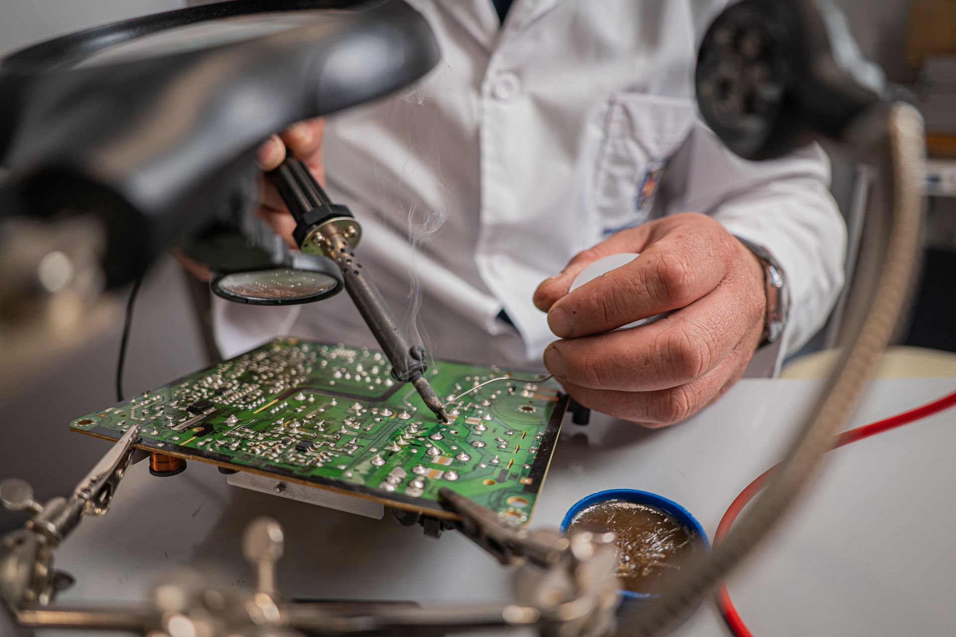
Small layout decisions can create significant soldering and placement problems during SMT PCB assembly.
Insufficient component spacing can block pick-and-place nozzle access when placing neighboring parts. Taller components may also shadow smaller ones during certain soldering processes, creating uneven heating.
Incorrect land patterns introduce another problem. On an 0402 component, one pad may wet before the other, pulling the component upright during reflow. This defect, called tombstoning, leaves an open connection. Poor pad geometry can also produce weak solder joints that fail during thermal cycling.
Thermal relief design affects soldering behavior, too. Connecting one SMD pad directly to a large ground pour increases its thermal mass. That pad heats more slowly than its neighbor, creating uneven wetting forces and another potential tombstoning condition.
Correcting these details protects assembly yield and long-term reliability.
How DFM PCB Panelization Affects Assembly and Handling
Panelization groups circuit boards into larger manufacturing panels, increasing SMT throughput and stencil efficiency.
Conveyor systems typically need approximately 3–5 mm of edge-rail clearance, depending on equipment specifications. Global fiducials establish panel alignment, while local fiducials help placement machines position fine-pitch components. Tooling holes accommodate fixtures and handling equipment.
Depanelization methods also influence layout decisions:
- V-scoring: Straight separation lines suit rectangular boards with adequate edge clearance.
- Tab routing: Routed outlines accommodate irregular board shapes and provide a smoother routed board edge compared to V-scoring.
- Mouse bites: Perforated tabs connect boards until separation, potentially leaving rough edges in the area where they’re placed. Mouse bites are generally used with a routed board edge.
Assemblers often develop the final panel arrangement, but designers must leave room for handling and separation.
Inefficient panelization can increase manual handling, reduce throughput, and raise per-unit assembly costs.
Designing PCBs for AOI, X-Ray, and Electrical Testing
Inspection accessibility should influence PCB layout before manufacturing.
Automated optical inspection (AOI) uses cameras to detect visible placement and soldering defects. Clear silkscreen polarity markings and unobstructed component views help identify problems.
X-ray inspection examines hidden solder connections beneath BGAs and other bottom-terminated packages. Component placement and overlapping features can affect image interpretation.
Electrical and flying probe testing depend on accessible test points with sufficient probe clearance. Dedicated fixtures may also need contact points arranged to match probe geometry.
For IPC Class 2 and Class 3 builds, inadequate inspection access can prevent verification against specified acceptance requirements. Testability belongs in the design process.
DFM in PCB Design for IPC Class 2 and Class 3 Builds
IPC-A-610 defines electronic assembly acceptance criteria across three classes: Class 1 covers general electronics, Class 2 covers dedicated-service equipment such as industrial electronics, and Class 3 covers high-reliability applications, including certain medical, aerospace, and defense systems.
Class 3 applies stricter solder-joint acceptance criteria and rejects certain workmanship conditions permitted under Class 2. Solder fillet dimensions, component alignment, and visible joint defects may face tighter limits.
Manufacturing planning must account for thermal balancing, suitable pad geometry, controlled soldering processes, and inspection access. Thermal relief practices should follow applicable design specifications rather than a universal rule.
Documentation and component traceability become important when specified by customers or regulated programs. Engineers should establish inspection criteria, material records, and acceptance expectations before production.
Ninja Circuits lists IPC-A-610 and ITAR among its industry credentials. Defense projects may involve ITAR registration and additional handling requirements, which should be confirmed for each build.
Send Your Next Build to Ninja Circuits for a DFM Check
A smoother prototype starts with three steps: prepare complete PCB artwork, BOM, documentation, and placement files; review footprints, clearances, and inspection access; and resolve flagged concerns before fabrication begins.
Ninja Circuits specializes in quick-turn prototypes and short-run
PCB assembly, helping engineers move from design files to working hardware with fewer production surprises.
Ready to get your next prototype moving?
Contact Ninja Circuits to request a quote and discuss your build.
If you need it fast, call Ninja.
INDUSTRY INSIGHTS