INDUSTRY INSIGHTS
PCB Thermal Management: Designing for Heat Dissipation
SHARE POST
Effective PCB thermal management starts with creating a low-resistance path that moves heat away from hot components using thermal vias, copper, strategic component placement, and thermally conductive materials.
But good thermal design has to survive assembly. Solder voids, poor thermal-pad contact, reflow conditions, and repeated thermal cycling can weaken that heat path. The best results come from treating heat dissipation as both a PCB design and assembly problem.
Why PCB Thermal Management Matters in Modern Designs
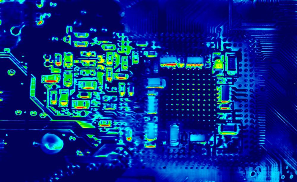
As boards get smaller and power density climbs, heat has less room to spread before component temperatures rise. Excess heat can push ICs toward junction temperature limits, alter electrical performance, shorten component life, and contribute to solder-joint fatigue or premature board failure. These concerns become especially important in compact power electronics, industrial controls, robotics, and automotive PCB assembly, where operating temperatures and thermal cycling can be severe.
Good thermal planning starts with identifying where heat originates and where it can realistically go. That means considering the complete path from the component package through the PCB and into the surrounding environment.
Common Heat Sources on a Populated PCB
Heat rarely comes from one place. Finding the biggest contributors helps engineers focus cooling efforts where they have the greatest effect. Common sources include:
- Power components: MOSFETs, voltage regulators, power ICs, and converters can generate concentrated hot spots during operation.
- Processors and FPGAs: High processing loads can produce substantial heat in a relatively small footprint.
- High-current paths: Resistance in traces, vias, connectors, and other conductors generates heat as current rises.
- Power passives: Resistors, inductors, and transformers can dissipate meaningful power, especially in converters, power supplies, and high-current circuits.
- Component clusters: Several warm components placed close together can raise the local board temperature, leaving each device with less temperature margin.
Identifying these sources early helps pinpoint where stronger thermal paths are needed.
Design Techniques for PCB Heat Dissipation
Effective PCB heat dissipation depends on giving heat practical routes away from hot components. In
high-tech PCB assembly, three layout choices have an especially large impact: thermal vias, copper distribution, and component placement.
Thermal Vias and Via Farms
Thermal vias create vertical paths that carry heat from a component’s exposed pad into internal or opposite-side copper. Grouping them into via farms can spread concentrated heat across a larger board area or toward a heat sink. Via diameter, spacing, plating, and fill strategy all influence performance and manufacturability. Vias placed directly beneath thermal pads also need assembly consideration. Poorly planned openings can draw solder away from the pad, contributing to uneven solder coverage or voiding and weakening the intended thermal connection.
Copper Pours and Heavy Copper Layers
Copper spreads heat laterally far better than standard PCB substrate materials, so larger pours and planes can reduce concentrated hot spots around power components. Increasing copper weight can also lower resistance in high-current paths, reducing heat generated by conductor losses. The tradeoff appears during assembly: large copper areas and heavy copper increase thermal mass and can pull heat away from solder joints during reflow. Copper should therefore be sized around the operating heat path while accounting for how the assembled board will heat during soldering.
Strategic Component Placement
Component placement determines how heat develops across the board before vias, copper, or cooling hardware come into play. Separating high-power devices can prevent overlapping hot zones, while placing heat-generating components near useful copper areas, airflow, or chassis connections creates shorter paths toward cooler regions. Placement also needs to account for nearby temperature-sensitive parts. Crowding a regulator, processor, and other warm devices into one area can raise local board temperature and reduce thermal margin, even when each component stays within its individual power rating.100+100+100+100
Materials That Move Heat: Substrates and TIMs
Standard FR-4 works for many boards, but higher power densities can expose its limited thermal conductivity. When the substrate becomes part of the bottleneck, material selection can create a more effective path away from hot components.
- Thermally conductive substrates: Metal-core boards, ceramics, and higher-conductivity laminates can move or spread heat more effectively than conventional FR-4. The right choice depends on electrical isolation, routing, mechanical, and fabrication constraints.
- Thermal interface materials (TIMs): Pads, films, and compounds fill microscopic gaps between a PCB or component and a heat sink or chassis, reducing interface resistance.
Material changes work best when they address the actual bottleneck rather than compensate for a weak thermal path elsewhere.
Assembly-Side Consequences of Thermal Stress
A strong thermal layout can lose effectiveness during SMT PCB assembly. Voids beneath QFNs and BGAs can interrupt heat transfer through soldered interfaces, while poorly planned thermal vias may draw solder away from exposed pads. Reflow conditions also matter because heavy copper and large thermal masses change how different areas of the board heat and cool.
Thermal stress continues after production. Repeated heating and cooling cause board materials, packages, and solder joints to expand and contract at different rates. Over many cycles, that strain can contribute to solder-joint fatigue, cracking, or intermittent failures. Thermal performance therefore depends on both the layout and the integrity of the finished assembly.
When to Loop In Your PCB Assembly Partner
Thermal decisions can affect manufacturability long before components reach the assembly line. Bringing an assembly partner into the conversation before the design is frozen creates time to review via-in-pad structures, exposed thermal pads, heavy copper, and unusual materials for potential build concerns.
From there, the assembly team can evaluate stencil strategy, solder volume, and reflow considerations around high-thermal-mass areas. Once prototypes are built, inspection of hidden joints and thermal testing can reveal gaps between predicted and actual performance. Addressing these details early can reduce avoidable revisions and help the next prototype reach the bench with fewer thermal unknowns.
Ready to Prototype a Thermally-Managed PCB?

Thermal performance becomes much easier to evaluate once a design moves from simulation to working hardware. A prototype can reveal hot spots, solder-interface concerns, and other differences between predicted temperatures and real operating conditions. That feedback creates a clearer path for refining the design before short-run or larger-scale production.
Ninja Circuits specializes in quick-turn prototypes and
PCB assembly, helping engineering teams move from design files to assembled boards without unnecessary delays. When thermal performance is one of the remaining questions, getting working hardware on the bench sooner can keep development moving.
Contact us to start your prototype. If you need it fast, call Ninja.

INDUSTRY INSIGHTS